1. Product Residences and Structural Honesty
1.1 Innate Attributes of Silicon Carbide
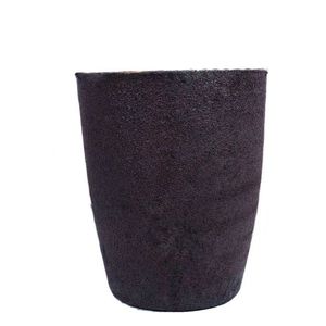
(Silicon Carbide Crucibles)
Silicon carbide (SiC) is a covalent ceramic substance made up of silicon and carbon atoms set up in a tetrahedral lattice framework, primarily existing in over 250 polytypic types, with 6H, 4H, and 3C being the most technically appropriate.
Its solid directional bonding imparts exceptional hardness (Mohs ~ 9.5), high thermal conductivity (80– 120 W/(m · K )for pure single crystals), and exceptional chemical inertness, making it one of one of the most robust materials for extreme environments.
The wide bandgap (2.9– 3.3 eV) guarantees excellent electric insulation at room temperature level and high resistance to radiation damage, while its reduced thermal growth coefficient (~ 4.0 × 10 ⁻⁶/ K) contributes to remarkable thermal shock resistance.
These innate residential or commercial properties are preserved even at temperature levels surpassing 1600 ° C, allowing SiC to maintain architectural stability under extended exposure to molten metals, slags, and reactive gases.
Unlike oxide porcelains such as alumina, SiC does not respond readily with carbon or kind low-melting eutectics in reducing environments, a crucial advantage in metallurgical and semiconductor processing.
When produced into crucibles– vessels developed to have and heat materials– SiC outshines standard products like quartz, graphite, and alumina in both life-span and procedure reliability.
1.2 Microstructure and Mechanical Stability
The efficiency of SiC crucibles is carefully connected to their microstructure, which depends upon the production method and sintering additives made use of.
Refractory-grade crucibles are generally generated via reaction bonding, where permeable carbon preforms are infiltrated with liquified silicon, developing β-SiC via the reaction Si(l) + C(s) → SiC(s).
This procedure yields a composite structure of primary SiC with recurring cost-free silicon (5– 10%), which improves thermal conductivity yet may restrict usage above 1414 ° C(the melting factor of silicon).
Additionally, fully sintered SiC crucibles are made via solid-state or liquid-phase sintering utilizing boron and carbon or alumina-yttria additives, attaining near-theoretical thickness and higher pureness.
These display superior creep resistance and oxidation stability however are much more expensive and tough to make in large sizes.
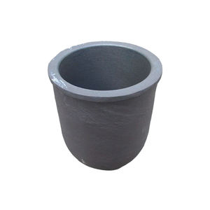
( Silicon Carbide Crucibles)
The fine-grained, interlacing microstructure of sintered SiC gives outstanding resistance to thermal tiredness and mechanical erosion, crucial when handling liquified silicon, germanium, or III-V substances in crystal growth processes.
Grain boundary design, consisting of the control of additional phases and porosity, plays an essential duty in figuring out long-lasting toughness under cyclic heating and hostile chemical environments.
2. Thermal Performance and Environmental Resistance
2.1 Thermal Conductivity and Warmth Distribution
Among the defining benefits of SiC crucibles is their high thermal conductivity, which enables quick and uniform heat transfer during high-temperature handling.
In contrast to low-conductivity materials like merged silica (1– 2 W/(m · K)), SiC effectively distributes thermal power throughout the crucible wall, minimizing local locations and thermal slopes.
This harmony is essential in processes such as directional solidification of multicrystalline silicon for photovoltaics, where temperature level homogeneity directly impacts crystal top quality and issue thickness.
The mix of high conductivity and reduced thermal development leads to an incredibly high thermal shock specification (R = k(1 − ν)α/ σ), making SiC crucibles immune to breaking throughout rapid home heating or cooling down cycles.
This allows for faster furnace ramp prices, improved throughput, and reduced downtime due to crucible failing.
Furthermore, the material’s capacity to stand up to repeated thermal biking without considerable destruction makes it suitable for set handling in industrial heating systems running above 1500 ° C.
2.2 Oxidation and Chemical Compatibility
At raised temperatures in air, SiC undergoes easy oxidation, developing a protective layer of amorphous silica (SiO TWO) on its surface: SiC + 3/2 O TWO → SiO TWO + CO.
This glazed layer densifies at high temperatures, functioning as a diffusion barrier that slows down further oxidation and maintains the underlying ceramic framework.
Nonetheless, in lowering ambiences or vacuum conditions– typical in semiconductor and steel refining– oxidation is subdued, and SiC continues to be chemically secure against liquified silicon, aluminum, and several slags.
It stands up to dissolution and reaction with molten silicon up to 1410 ° C, although prolonged exposure can cause small carbon pick-up or interface roughening.
Crucially, SiC does not introduce metallic pollutants into delicate thaws, a vital need for electronic-grade silicon production where contamination by Fe, Cu, or Cr must be maintained listed below ppb degrees.
Nevertheless, care should be taken when refining alkaline planet metals or extremely reactive oxides, as some can wear away SiC at severe temperature levels.
3. Production Processes and Quality Control
3.1 Manufacture Techniques and Dimensional Control
The manufacturing of SiC crucibles includes shaping, drying, and high-temperature sintering or infiltration, with techniques selected based on required purity, size, and application.
Usual developing techniques include isostatic pressing, extrusion, and slide spreading, each providing different levels of dimensional precision and microstructural harmony.
For big crucibles utilized in photovoltaic ingot spreading, isostatic pressing makes certain consistent wall density and density, decreasing the risk of uneven thermal growth and failure.
Reaction-bonded SiC (RBSC) crucibles are cost-effective and extensively utilized in factories and solar markets, though recurring silicon restrictions optimal solution temperature level.
Sintered SiC (SSiC) variations, while more expensive, offer premium purity, strength, and resistance to chemical attack, making them ideal for high-value applications like GaAs or InP crystal development.
Accuracy machining after sintering may be needed to achieve limited tolerances, especially for crucibles used in upright slope freeze (VGF) or Czochralski (CZ) systems.
Surface area finishing is crucial to reduce nucleation sites for issues and guarantee smooth thaw flow during spreading.
3.2 Quality Assurance and Efficiency Recognition
Rigorous quality control is necessary to guarantee integrity and durability of SiC crucibles under requiring operational conditions.
Non-destructive evaluation techniques such as ultrasonic testing and X-ray tomography are employed to spot internal cracks, voids, or density variations.
Chemical evaluation by means of XRF or ICP-MS confirms reduced levels of metal impurities, while thermal conductivity and flexural strength are gauged to confirm material uniformity.
Crucibles are usually based on substitute thermal biking tests before shipment to identify prospective failure settings.
Set traceability and qualification are typical in semiconductor and aerospace supply chains, where element failing can bring about expensive manufacturing losses.
4. Applications and Technological Influence
4.1 Semiconductor and Photovoltaic Industries
Silicon carbide crucibles play a pivotal function in the production of high-purity silicon for both microelectronics and solar batteries.
In directional solidification furnaces for multicrystalline photovoltaic or pv ingots, huge SiC crucibles act as the primary container for molten silicon, withstanding temperatures above 1500 ° C for several cycles.
Their chemical inertness prevents contamination, while their thermal stability guarantees consistent solidification fronts, bring about higher-quality wafers with fewer dislocations and grain limits.
Some producers layer the inner surface with silicon nitride or silica to additionally decrease attachment and promote ingot release after cooling down.
In research-scale Czochralski growth of compound semiconductors, smaller sized SiC crucibles are used to hold thaws of GaAs, InSb, or CdTe, where marginal sensitivity and dimensional stability are extremely important.
4.2 Metallurgy, Shop, and Emerging Technologies
Beyond semiconductors, SiC crucibles are vital in metal refining, alloy preparation, and laboratory-scale melting procedures entailing aluminum, copper, and precious metals.
Their resistance to thermal shock and erosion makes them ideal for induction and resistance heating systems in shops, where they last longer than graphite and alumina alternatives by numerous cycles.
In additive production of responsive steels, SiC containers are made use of in vacuum cleaner induction melting to avoid crucible failure and contamination.
Emerging applications include molten salt activators and focused solar energy systems, where SiC vessels may consist of high-temperature salts or liquid metals for thermal power storage space.
With continuous developments in sintering technology and covering engineering, SiC crucibles are poised to support next-generation materials processing, enabling cleaner, more effective, and scalable commercial thermal systems.
In recap, silicon carbide crucibles stand for a crucial allowing innovation in high-temperature material synthesis, combining phenomenal thermal, mechanical, and chemical performance in a solitary engineered part.
Their widespread fostering throughout semiconductor, solar, and metallurgical sectors emphasizes their duty as a foundation of contemporary industrial ceramics.
5. Distributor
Advanced Ceramics founded on October 17, 2012, is a high-tech enterprise committed to the research and development, production, processing, sales and technical services of ceramic relative materials and products. Our products includes but not limited to Boron Carbide Ceramic Products, Boron Nitride Ceramic Products, Silicon Carbide Ceramic Products, Silicon Nitride Ceramic Products, Zirconium Dioxide Ceramic Products, etc. If you are interested, please feel free to contact us.
Tags: Silicon Carbide Crucibles, Silicon Carbide Ceramic, Silicon Carbide Ceramic Crucibles
All articles and pictures are from the Internet. If there are any copyright issues, please contact us in time to delete.
Inquiry us