1. Crystal Framework and Polytypism of Silicon Carbide
1.1 Cubic and Hexagonal Polytypes: From 3C to 6H and Past
(Silicon Carbide Ceramics)
Silicon carbide (SiC) is a covalently adhered ceramic composed of silicon and carbon atoms set up in a tetrahedral control, creating one of one of the most complicated systems of polytypism in materials scientific research.
Unlike most porcelains with a single secure crystal framework, SiC exists in over 250 recognized polytypes– distinct stacking series of close-packed Si-C bilayers along the c-axis– ranging from cubic 3C-SiC (also called β-SiC) to hexagonal 6H-SiC and rhombohedral 15R-SiC.
The most common polytypes used in engineering applications are 3C (cubic), 4H, and 6H (both hexagonal), each exhibiting a little different electronic band structures and thermal conductivities.
3C-SiC, with its zinc blende framework, has the narrowest bandgap (~ 2.3 eV) and is typically expanded on silicon substratums for semiconductor tools, while 4H-SiC supplies premium electron flexibility and is liked for high-power electronic devices.
The strong covalent bonding and directional nature of the Si– C bond provide exceptional solidity, thermal security, and resistance to creep and chemical assault, making SiC suitable for severe atmosphere applications.
1.2 Issues, Doping, and Digital Properties
In spite of its architectural complexity, SiC can be doped to achieve both n-type and p-type conductivity, enabling its usage in semiconductor gadgets.
Nitrogen and phosphorus serve as donor contaminations, presenting electrons right into the transmission band, while light weight aluminum and boron serve as acceptors, producing holes in the valence band.
However, p-type doping effectiveness is limited by high activation powers, particularly in 4H-SiC, which positions challenges for bipolar device design.
Indigenous defects such as screw dislocations, micropipes, and stacking mistakes can break down gadget efficiency by functioning as recombination centers or leakage paths, demanding high-grade single-crystal development for electronic applications.
The vast bandgap (2.3– 3.3 eV depending on polytype), high malfunction electrical area (~ 3 MV/cm), and outstanding thermal conductivity (~ 3– 4 W/m · K for 4H-SiC) make SiC far above silicon in high-temperature, high-voltage, and high-frequency power electronics.
2. Handling and Microstructural Design
( Silicon Carbide Ceramics)
2.1 Sintering and Densification Strategies
Silicon carbide is naturally hard to densify as a result of its strong covalent bonding and low self-diffusion coefficients, calling for advanced handling methods to attain full thickness without additives or with very little sintering aids.
Pressureless sintering of submicron SiC powders is possible with the addition of boron and carbon, which advertise densification by eliminating oxide layers and enhancing solid-state diffusion.
Hot pushing applies uniaxial stress during heating, enabling complete densification at reduced temperature levels (~ 1800– 2000 ° C )and creating fine-grained, high-strength components ideal for reducing tools and use components.
For large or complicated forms, reaction bonding is used, where permeable carbon preforms are infiltrated with liquified silicon at ~ 1600 ° C, creating β-SiC in situ with marginal contraction.
Nevertheless, residual totally free silicon (~ 5– 10%) continues to be in the microstructure, restricting high-temperature efficiency and oxidation resistance over 1300 ° C.
2.2 Additive Production and Near-Net-Shape Construction
Recent breakthroughs in additive production (AM), particularly binder jetting and stereolithography utilizing SiC powders or preceramic polymers, make it possible for the fabrication of intricate geometries previously unattainable with conventional methods.
In polymer-derived ceramic (PDC) courses, liquid SiC precursors are shaped using 3D printing and after that pyrolyzed at heats to yield amorphous or nanocrystalline SiC, frequently calling for further densification.
These strategies decrease machining prices and product waste, making SiC a lot more available for aerospace, nuclear, and warm exchanger applications where detailed layouts boost efficiency.
Post-processing actions such as chemical vapor seepage (CVI) or liquid silicon infiltration (LSI) are sometimes utilized to boost thickness and mechanical stability.
3. Mechanical, Thermal, and Environmental Efficiency
3.1 Strength, Hardness, and Put On Resistance
Silicon carbide ranks among the hardest recognized products, with a Mohs solidity of ~ 9.5 and Vickers solidity going beyond 25 GPa, making it extremely immune to abrasion, disintegration, and damaging.
Its flexural stamina generally varies from 300 to 600 MPa, depending on handling approach and grain dimension, and it maintains strength at temperatures as much as 1400 ° C in inert environments.
Fracture durability, while moderate (~ 3– 4 MPa · m ¹/ ²), is sufficient for many structural applications, especially when integrated with fiber support in ceramic matrix composites (CMCs).
SiC-based CMCs are made use of in generator blades, combustor linings, and brake systems, where they provide weight financial savings, gas performance, and prolonged life span over metal counterparts.
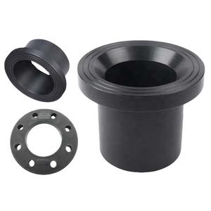
Its excellent wear resistance makes SiC suitable for seals, bearings, pump parts, and ballistic armor, where longevity under harsh mechanical loading is essential.
3.2 Thermal Conductivity and Oxidation Security
One of SiC’s most useful residential properties is its high thermal conductivity– up to 490 W/m · K for single-crystal 4H-SiC and ~ 30– 120 W/m · K for polycrystalline kinds– surpassing that of several metals and enabling effective warmth dissipation.
This property is vital in power electronic devices, where SiC devices generate less waste warmth and can run at greater power thickness than silicon-based tools.
At elevated temperature levels in oxidizing settings, SiC forms a protective silica (SiO ₂) layer that reduces more oxidation, supplying great ecological sturdiness as much as ~ 1600 ° C.
However, in water vapor-rich environments, this layer can volatilize as Si(OH)₄, bring about sped up deterioration– a vital challenge in gas turbine applications.
4. Advanced Applications in Power, Electronic Devices, and Aerospace
4.1 Power Electronic Devices and Semiconductor Gadgets
Silicon carbide has reinvented power electronic devices by allowing devices such as Schottky diodes, MOSFETs, and JFETs that operate at higher voltages, frequencies, and temperatures than silicon equivalents.
These devices lower power losses in electric automobiles, renewable resource inverters, and industrial motor drives, adding to worldwide energy efficiency renovations.
The capability to run at joint temperatures over 200 ° C allows for simplified cooling systems and raised system dependability.
Moreover, SiC wafers are made use of as substratums for gallium nitride (GaN) epitaxy in high-electron-mobility transistors (HEMTs), combining the benefits of both wide-bandgap semiconductors.
4.2 Nuclear, Aerospace, and Optical Solutions
In atomic power plants, SiC is a key part of accident-tolerant fuel cladding, where its reduced neutron absorption cross-section, radiation resistance, and high-temperature stamina boost safety and efficiency.
In aerospace, SiC fiber-reinforced compounds are utilized in jet engines and hypersonic vehicles for their lightweight and thermal stability.
In addition, ultra-smooth SiC mirrors are employed in space telescopes as a result of their high stiffness-to-density ratio, thermal security, and polishability to sub-nanometer roughness.
In summary, silicon carbide porcelains stand for a foundation of modern-day advanced materials, integrating remarkable mechanical, thermal, and digital residential or commercial properties.
With exact control of polytype, microstructure, and handling, SiC continues to enable technical developments in power, transport, and extreme environment design.
5. Provider
TRUNNANO is a supplier of Spherical Tungsten Powder with over 12 years of experience in nano-building energy conservation and nanotechnology development. It accepts payment via Credit Card, T/T, West Union and Paypal. Trunnano will ship the goods to customers overseas through FedEx, DHL, by air, or by sea. If you want to know more about Spherical Tungsten Powder, please feel free to contact us and send an inquiry(sales5@nanotrun.com).
Tags: silicon carbide ceramic,silicon carbide ceramic products, industry ceramic
All articles and pictures are from the Internet. If there are any copyright issues, please contact us in time to delete.
Inquiry us